24/10/2024 12:52
Naively I tried adding a "DDR3 Writer" IP block to the working ddr3 pcie design. It didn't work (more details below). Instead of making a new project, I built on top of the existing, so I had to waste some time rebuilidng the project.
The point of this note is just to say that somehow adding the blocks, then removing and reconnecting screwed something up. Particularly, I tried playing with the MIG IP block, which I think renamed it's IP block somehow in vivado; then vivado could not longer find the board files that configure it.
It seems just rebuilding the project from scratch worked.
24/10/2024 13:40
I created a new module AXI module in vivado, loosely following some steps in this manual.
I wanted to write a AXI IP block that just writes an incrimneting number to one register in the DDR3 RAM every second (I chose the 0x0000_0000 address for this). I assume the given clock is a 250 MHz clock for this.
The only extra logic I added was the following state machine:
    // Add user logic here

    // Parameters for state machine states
    localparam IDLE = 2'b00, INIT_WRITE = 2'b01, WAIT_WRITE = 2'b10;

    // Register for current state
    reg [1:0] state;

    // Counter for 1-second interval
    reg [31:0] second_counter;

    // Counter for data to write
    reg [31:0] write_data_counter;

    // AXI write address and data
    reg [C_M00_AXI_ADDR_WIDTH-1 : 0] axi_awaddr;
    reg [C_M00_AXI_DATA_WIDTH-1 : 0] axi_wdata;
    reg axi_awvalid;
    reg axi_wvalid;

    // 250 MHz clock = 250 million cycles per second
    localparam ONE_SECOND_COUNT = 250_000_000;

    // AXI transaction done signal
    assign m00_axi_awvalid = axi_awvalid;
    assign m00_axi_wvalid  = axi_wvalid;
    assign m00_axi_awaddr  = axi_awaddr;
    assign m00_axi_wdata   = axi_wdata;

    // Main state machine
    always @(posedge m00_axi_aclk) begin
        if (!m00_axi_aresetn) begin
            state <= IDLE;
            second_counter <= 0;
            write_data_counter <= 0;
            axi_awvalid <= 0;
            axi_wvalid <= 0;
        end else begin
            case (state)
                IDLE: begin
                    if (second_counter == ONE_SECOND_COUNT - 1) begin
                        // Trigger write operation every second
                        axi_awaddr <= C_M00_AXI_TARGET_SLAVE_BASE_ADDR; // Target register address
                        axi_wdata <= write_data_counter; // Write incrementing data
                        axi_awvalid <= 1;
                        axi_wvalid <= 1;
                        second_counter <= 0; // Reset second counter
                        write_data_counter <= write_data_counter + 1; // Increment data to be written
                        state <= INIT_WRITE;
                    end else begin
                        second_counter <= second_counter + 1;
                    end
                end

                INIT_WRITE: begin
                    if (m00_axi_awready && m00_axi_wready) begin
                        axi_awvalid <= 0;
                        axi_wvalid <= 0;
                        state <= WAIT_WRITE;
                    end
                end

                WAIT_WRITE: begin
                    if (m00_axi_bvalid) begin
                        // Write complete, back to idle
                        state <= IDLE;
                    end
                end

                default: state <= IDLE;
            endcase
        end
    end

    // User logic ends
// Add user logic here
// Parameters for state machine states
localparam IDLE = 2'b00, INIT_WRITE = 2'b01, WAIT_WRITE = 2'b10;
// Register for current state
reg [1:0] state;
// Counter for 1-second interval
reg [31:0] second_counter;
// Counter for data to write
reg [31:0] write_data_counter;
// AXI write address and data
reg [C_M00_AXI_ADDR_WIDTH-1 : 0] axi_awaddr;
reg [C_M00_AXI_DATA_WIDTH-1 : 0] axi_wdata;
reg axi_awvalid;
reg axi_wvalid;
// 250 MHz clock = 250 million cycles per second
localparam ONE_SECOND_COUNT = 250_000_000;
// AXI transaction done signal
assign m00_axi_awvalid = axi_awvalid;
assign m00_axi_wvalid = axi_wvalid;
assign m00_axi_awaddr = axi_awaddr;
assign m00_axi_wdata = axi_wdata;
// Main state machine
always @(posedge m00_axi_aclk) begin
if (!m00_axi_aresetn) begin
state <= IDLE;
second_counter <= 0;
write_data_counter <= 0;
axi_awvalid <= 0;
axi_wvalid <= 0;
end else begin
case (state)
IDLE: begin
if (second_counter == ONE_SECOND_COUNT - 1) begin
// Trigger write operation every second
axi_awaddr <= C_M00_AXI_TARGET_SLAVE_BASE_ADDR; // Target register address
axi_wdata <= write_data_counter; // Write incrementing data
axi_awvalid <= 1;
axi_wvalid <= 1;
second_counter <= 0; // Reset second counter
write_data_counter <= write_data_counter + 1; // Increment data to be written
state <= INIT_WRITE;
end else begin
second_counter <= second_counter + 1;
end
end
INIT_WRITE: begin
if (m00_axi_awready && m00_axi_wready) begin
axi_awvalid <= 0;
axi_wvalid <= 0;
state <= WAIT_WRITE;
end
end
WAIT_WRITE: begin
if (m00_axi_bvalid) begin
// Write complete, back to idle
state <= IDLE;
end
end
default: state <= IDLE;
endcase
end
end
// User logic endsAnd the full file looks like this (everything else automatically generated by Vivado):
`timescale 1 ns / 1 ps
module AXI_DDR3_Writer_v1_0 #
(
// Users to add parameters here
// User parameters ends
// Do not modify the parameters beyond this line
// Parameters of Axi Master Bus Interface M00_AXI
parameter C_M00_AXI_TARGET_SLAVE_BASE_ADDR = 32'h00000000,
parameter integer C_M00_AXI_BURST_LEN = 16,
parameter integer C_M00_AXI_ID_WIDTH = 1,
parameter integer C_M00_AXI_ADDR_WIDTH = 32,
parameter integer C_M00_AXI_DATA_WIDTH = 32,
parameter integer C_M00_AXI_AWUSER_WIDTH = 0,
parameter integer C_M00_AXI_ARUSER_WIDTH = 0,
parameter integer C_M00_AXI_WUSER_WIDTH = 32,
parameter integer C_M00_AXI_RUSER_WIDTH = 32,
parameter integer C_M00_AXI_BUSER_WIDTH = 0
)
(
// Users to add ports here
// User ports ends
// Do not modify the ports beyond this line
// Ports of Axi Master Bus Interface M00_AXI
input wire m00_axi_init_axi_txn,
output wire m00_axi_txn_done,
output wire m00_axi_error,
input wire m00_axi_aclk,
input wire m00_axi_aresetn,
output wire [C_M00_AXI_ID_WIDTH-1 : 0] m00_axi_awid,
output wire [C_M00_AXI_ADDR_WIDTH-1 : 0] m00_axi_awaddr,
output wire [7 : 0] m00_axi_awlen,
output wire [2 : 0] m00_axi_awsize,
output wire [1 : 0] m00_axi_awburst,
output wire m00_axi_awlock,
output wire [3 : 0] m00_axi_awcache,
output wire [2 : 0] m00_axi_awprot,
output wire [3 : 0] m00_axi_awqos,
output wire [C_M00_AXI_AWUSER_WIDTH-1 : 0] m00_axi_awuser,
output wire m00_axi_awvalid,
input wire m00_axi_awready,
output wire [C_M00_AXI_DATA_WIDTH-1 : 0] m00_axi_wdata,
output wire [C_M00_AXI_DATA_WIDTH/8-1 : 0] m00_axi_wstrb,
output wire m00_axi_wlast,
output wire [C_M00_AXI_WUSER_WIDTH-1 : 0] m00_axi_wuser,
output wire m00_axi_wvalid,
input wire m00_axi_wready,
input wire [C_M00_AXI_ID_WIDTH-1 : 0] m00_axi_bid,
input wire [1 : 0] m00_axi_bresp,
input wire [C_M00_AXI_BUSER_WIDTH-1 : 0] m00_axi_buser,
input wire m00_axi_bvalid,
output wire m00_axi_bready,
output wire [C_M00_AXI_ID_WIDTH-1 : 0] m00_axi_arid,
output wire [C_M00_AXI_ADDR_WIDTH-1 : 0] m00_axi_araddr,
output wire [7 : 0] m00_axi_arlen,
output wire [2 : 0] m00_axi_arsize,
output wire [1 : 0] m00_axi_arburst,
output wire m00_axi_arlock,
output wire [3 : 0] m00_axi_arcache,
output wire [2 : 0] m00_axi_arprot,
output wire [3 : 0] m00_axi_arqos,
output wire [C_M00_AXI_ARUSER_WIDTH-1 : 0] m00_axi_aruser,
output wire m00_axi_arvalid,
input wire m00_axi_arready,
input wire [C_M00_AXI_ID_WIDTH-1 : 0] m00_axi_rid,
input wire [C_M00_AXI_DATA_WIDTH-1 : 0] m00_axi_rdata,
input wire [1 : 0] m00_axi_rresp,
input wire m00_axi_rlast,
input wire [C_M00_AXI_RUSER_WIDTH-1 : 0] m00_axi_ruser,
input wire m00_axi_rvalid,
output wire m00_axi_rready
);
// Instantiation of Axi Bus Interface M00_AXI
AXI_DDR3_Writer_v1_0_M00_AXI # (
.C_M_TARGET_SLAVE_BASE_ADDR(C_M00_AXI_TARGET_SLAVE_BASE_ADDR),
.C_M_AXI_BURST_LEN(C_M00_AXI_BURST_LEN),
.C_M_AXI_ID_WIDTH(C_M00_AXI_ID_WIDTH),
.C_M_AXI_ADDR_WIDTH(C_M00_AXI_ADDR_WIDTH),
.C_M_AXI_DATA_WIDTH(C_M00_AXI_DATA_WIDTH),
.C_M_AXI_AWUSER_WIDTH(C_M00_AXI_AWUSER_WIDTH),
.C_M_AXI_ARUSER_WIDTH(C_M00_AXI_ARUSER_WIDTH),
.C_M_AXI_WUSER_WIDTH(C_M00_AXI_WUSER_WIDTH),
.C_M_AXI_RUSER_WIDTH(C_M00_AXI_RUSER_WIDTH),
.C_M_AXI_BUSER_WIDTH(C_M00_AXI_BUSER_WIDTH)
) AXI_DDR3_Writer_v1_0_M00_AXI_inst (
.INIT_AXI_TXN(m00_axi_init_axi_txn),
.TXN_DONE(m00_axi_txn_done),
.ERROR(m00_axi_error),
.M_AXI_ACLK(m00_axi_aclk),
.M_AXI_ARESETN(m00_axi_aresetn),
.M_AXI_AWID(m00_axi_awid),
.M_AXI_AWADDR(m00_axi_awaddr),
.M_AXI_AWLEN(m00_axi_awlen),
.M_AXI_AWSIZE(m00_axi_awsize),
.M_AXI_AWBURST(m00_axi_awburst),
.M_AXI_AWLOCK(m00_axi_awlock),
.M_AXI_AWCACHE(m00_axi_awcache),
.M_AXI_AWPROT(m00_axi_awprot),
.M_AXI_AWQOS(m00_axi_awqos),
.M_AXI_AWUSER(m00_axi_awuser),
.M_AXI_AWVALID(m00_axi_awvalid),
.M_AXI_AWREADY(m00_axi_awready),
.M_AXI_WDATA(m00_axi_wdata),
.M_AXI_WSTRB(m00_axi_wstrb),
.M_AXI_WLAST(m00_axi_wlast),
.M_AXI_WUSER(m00_axi_wuser),
.M_AXI_WVALID(m00_axi_wvalid),
.M_AXI_WREADY(m00_axi_wready),
.M_AXI_BID(m00_axi_bid),
.M_AXI_BRESP(m00_axi_bresp),
.M_AXI_BUSER(m00_axi_buser),
.M_AXI_BVALID(m00_axi_bvalid),
.M_AXI_BREADY(m00_axi_bready),
.M_AXI_ARID(m00_axi_arid),
.M_AXI_ARADDR(m00_axi_araddr),
.M_AXI_ARLEN(m00_axi_arlen),
.M_AXI_ARSIZE(m00_axi_arsize),
.M_AXI_ARBURST(m00_axi_arburst),
.M_AXI_ARLOCK(m00_axi_arlock),
.M_AXI_ARCACHE(m00_axi_arcache),
.M_AXI_ARPROT(m00_axi_arprot),
.M_AXI_ARQOS(m00_axi_arqos),
.M_AXI_ARUSER(m00_axi_aruser),
.M_AXI_ARVALID(m00_axi_arvalid),
.M_AXI_ARREADY(m00_axi_arready),
.M_AXI_RID(m00_axi_rid),
.M_AXI_RDATA(m00_axi_rdata),
.M_AXI_RRESP(m00_axi_rresp),
.M_AXI_RLAST(m00_axi_rlast),
.M_AXI_RUSER(m00_axi_ruser),
.M_AXI_RVALID(m00_axi_rvalid),
.M_AXI_RREADY(m00_axi_rready)
);
    // Add user logic here

    // Parameters for state machine states
    localparam IDLE = 2'b00, INIT_WRITE = 2'b01, WAIT_WRITE = 2'b10;

    // Register for current state
    reg [1:0] state;

    // Counter for 1-second interval
    reg [31:0] second_counter;

    // Counter for data to write
    reg [31:0] write_data_counter;

    // AXI write address and data
    reg [C_M00_AXI_ADDR_WIDTH-1 : 0] axi_awaddr;
    reg [C_M00_AXI_DATA_WIDTH-1 : 0] axi_wdata;
    reg axi_awvalid;
    reg axi_wvalid;

    // 250 MHz clock = 250 million cycles per second
    localparam ONE_SECOND_COUNT = 250_000_000;

    // AXI transaction done signal
    assign m00_axi_awvalid = axi_awvalid;
    assign m00_axi_wvalid  = axi_wvalid;
    assign m00_axi_awaddr  = axi_awaddr;
    assign m00_axi_wdata   = axi_wdata;

    // Main state machine
    always @(posedge m00_axi_aclk) begin
        if (!m00_axi_aresetn) begin
            state <= IDLE;
            second_counter <= 0;
            write_data_counter <= 0;
            axi_awvalid <= 0;
            axi_wvalid <= 0;
        end else begin
            case (state)
                IDLE: begin
                    if (second_counter == ONE_SECOND_COUNT - 1) begin
                        // Trigger write operation every second
                        axi_awaddr <= C_M00_AXI_TARGET_SLAVE_BASE_ADDR; // Target register address
                        axi_wdata <= write_data_counter; // Write incrementing data
                        axi_awvalid <= 1;
                        axi_wvalid <= 1;
                        second_counter <= 0; // Reset second counter
                        write_data_counter <= write_data_counter + 1; // Increment data to be written
                        state <= INIT_WRITE;
                    end else begin
                        second_counter <= second_counter + 1;
                    end
                end

                INIT_WRITE: begin
                    if (m00_axi_awready && m00_axi_wready) begin
                        axi_awvalid <= 0;
                        axi_wvalid <= 0;
                        state <= WAIT_WRITE;
                    end
                end

                WAIT_WRITE: begin
                    if (m00_axi_bvalid) begin
                        // Write complete, back to idle
                        state <= IDLE;
                    end
                end

                default: state <= IDLE;
            endcase
        end
    end

    // User logic ends
endmodule`timescale 1 ns / 1 ps
module AXI_DDR3_Writer_v1_0 #
(
// Users to add parameters here
// User parameters ends
// Do not modify the parameters beyond this line
// Parameters of Axi Master Bus Interface M00_AXI
parameter C_M00_AXI_TARGET_SLAVE_BASE_ADDR = 32'h00000000,
parameter integer C_M00_AXI_BURST_LEN = 16,
parameter integer C_M00_AXI_ID_WIDTH = 1,
parameter integer C_M00_AXI_ADDR_WIDTH = 32,
parameter integer C_M00_AXI_DATA_WIDTH = 32,
parameter integer C_M00_AXI_AWUSER_WIDTH = 0,
parameter integer C_M00_AXI_ARUSER_WIDTH = 0,
parameter integer C_M00_AXI_WUSER_WIDTH = 32,
parameter integer C_M00_AXI_RUSER_WIDTH = 32,
parameter integer C_M00_AXI_BUSER_WIDTH = 0
)
(
// Users to add ports here
// User ports ends
// Do not modify the ports beyond this line
// Ports of Axi Master Bus Interface M00_AXI
input wire m00_axi_init_axi_txn,
output wire m00_axi_txn_done,
output wire m00_axi_error,
input wire m00_axi_aclk,
input wire m00_axi_aresetn,
output wire [C_M00_AXI_ID_WIDTH-1 : 0] m00_axi_awid,
output wire [C_M00_AXI_ADDR_WIDTH-1 : 0] m00_axi_awaddr,
output wire [7 : 0] m00_axi_awlen,
output wire [2 : 0] m00_axi_awsize,
output wire [1 : 0] m00_axi_awburst,
output wire m00_axi_awlock,
output wire [3 : 0] m00_axi_awcache,
output wire [2 : 0] m00_axi_awprot,
output wire [3 : 0] m00_axi_awqos,
output wire [C_M00_AXI_AWUSER_WIDTH-1 : 0] m00_axi_awuser,
output wire m00_axi_awvalid,
input wire m00_axi_awready,
output wire [C_M00_AXI_DATA_WIDTH-1 : 0] m00_axi_wdata,
output wire [C_M00_AXI_DATA_WIDTH/8-1 : 0] m00_axi_wstrb,
output wire m00_axi_wlast,
output wire [C_M00_AXI_WUSER_WIDTH-1 : 0] m00_axi_wuser,
output wire m00_axi_wvalid,
input wire m00_axi_wready,
input wire [C_M00_AXI_ID_WIDTH-1 : 0] m00_axi_bid,
input wire [1 : 0] m00_axi_bresp,
input wire [C_M00_AXI_BUSER_WIDTH-1 : 0] m00_axi_buser,
input wire m00_axi_bvalid,
output wire m00_axi_bready,
output wire [C_M00_AXI_ID_WIDTH-1 : 0] m00_axi_arid,
output wire [C_M00_AXI_ADDR_WIDTH-1 : 0] m00_axi_araddr,
output wire [7 : 0] m00_axi_arlen,
output wire [2 : 0] m00_axi_arsize,
output wire [1 : 0] m00_axi_arburst,
output wire m00_axi_arlock,
output wire [3 : 0] m00_axi_arcache,
output wire [2 : 0] m00_axi_arprot,
output wire [3 : 0] m00_axi_arqos,
output wire [C_M00_AXI_ARUSER_WIDTH-1 : 0] m00_axi_aruser,
output wire m00_axi_arvalid,
input wire m00_axi_arready,
input wire [C_M00_AXI_ID_WIDTH-1 : 0] m00_axi_rid,
input wire [C_M00_AXI_DATA_WIDTH-1 : 0] m00_axi_rdata,
input wire [1 : 0] m00_axi_rresp,
input wire m00_axi_rlast,
input wire [C_M00_AXI_RUSER_WIDTH-1 : 0] m00_axi_ruser,
input wire m00_axi_rvalid,
output wire m00_axi_rready
);
// Instantiation of Axi Bus Interface M00_AXI
AXI_DDR3_Writer_v1_0_M00_AXI # (
.C_M_TARGET_SLAVE_BASE_ADDR(C_M00_AXI_TARGET_SLAVE_BASE_ADDR),
.C_M_AXI_BURST_LEN(C_M00_AXI_BURST_LEN),
.C_M_AXI_ID_WIDTH(C_M00_AXI_ID_WIDTH),
.C_M_AXI_ADDR_WIDTH(C_M00_AXI_ADDR_WIDTH),
.C_M_AXI_DATA_WIDTH(C_M00_AXI_DATA_WIDTH),
.C_M_AXI_AWUSER_WIDTH(C_M00_AXI_AWUSER_WIDTH),
.C_M_AXI_ARUSER_WIDTH(C_M00_AXI_ARUSER_WIDTH),
.C_M_AXI_WUSER_WIDTH(C_M00_AXI_WUSER_WIDTH),
.C_M_AXI_RUSER_WIDTH(C_M00_AXI_RUSER_WIDTH),
.C_M_AXI_BUSER_WIDTH(C_M00_AXI_BUSER_WIDTH)
) AXI_DDR3_Writer_v1_0_M00_AXI_inst (
.INIT_AXI_TXN(m00_axi_init_axi_txn),
.TXN_DONE(m00_axi_txn_done),
.ERROR(m00_axi_error),
.M_AXI_ACLK(m00_axi_aclk),
.M_AXI_ARESETN(m00_axi_aresetn),
.M_AXI_AWID(m00_axi_awid),
.M_AXI_AWADDR(m00_axi_awaddr),
.M_AXI_AWLEN(m00_axi_awlen),
.M_AXI_AWSIZE(m00_axi_awsize),
.M_AXI_AWBURST(m00_axi_awburst),
.M_AXI_AWLOCK(m00_axi_awlock),
.M_AXI_AWCACHE(m00_axi_awcache),
.M_AXI_AWPROT(m00_axi_awprot),
.M_AXI_AWQOS(m00_axi_awqos),
.M_AXI_AWUSER(m00_axi_awuser),
.M_AXI_AWVALID(m00_axi_awvalid),
.M_AXI_AWREADY(m00_axi_awready),
.M_AXI_WDATA(m00_axi_wdata),
.M_AXI_WSTRB(m00_axi_wstrb),
.M_AXI_WLAST(m00_axi_wlast),
.M_AXI_WUSER(m00_axi_wuser),
.M_AXI_WVALID(m00_axi_wvalid),
.M_AXI_WREADY(m00_axi_wready),
.M_AXI_BID(m00_axi_bid),
.M_AXI_BRESP(m00_axi_bresp),
.M_AXI_BUSER(m00_axi_buser),
.M_AXI_BVALID(m00_axi_bvalid),
.M_AXI_BREADY(m00_axi_bready),
.M_AXI_ARID(m00_axi_arid),
.M_AXI_ARADDR(m00_axi_araddr),
.M_AXI_ARLEN(m00_axi_arlen),
.M_AXI_ARSIZE(m00_axi_arsize),
.M_AXI_ARBURST(m00_axi_arburst),
.M_AXI_ARLOCK(m00_axi_arlock),
.M_AXI_ARCACHE(m00_axi_arcache),
.M_AXI_ARPROT(m00_axi_arprot),
.M_AXI_ARQOS(m00_axi_arqos),
.M_AXI_ARUSER(m00_axi_aruser),
.M_AXI_ARVALID(m00_axi_arvalid),
.M_AXI_ARREADY(m00_axi_arready),
.M_AXI_RID(m00_axi_rid),
.M_AXI_RDATA(m00_axi_rdata),
.M_AXI_RRESP(m00_axi_rresp),
.M_AXI_RLAST(m00_axi_rlast),
.M_AXI_RUSER(m00_axi_ruser),
.M_AXI_RVALID(m00_axi_rvalid),
.M_AXI_RREADY(m00_axi_rready)
);
// Add user logic here
// Parameters for state machine states
localparam IDLE = 2'b00, INIT_WRITE = 2'b01, WAIT_WRITE = 2'b10;
// Register for current state
reg [1:0] state;
// Counter for 1-second interval
reg [31:0] second_counter;
// Counter for data to write
reg [31:0] write_data_counter;
// AXI write address and data
reg [C_M00_AXI_ADDR_WIDTH-1 : 0] axi_awaddr;
reg [C_M00_AXI_DATA_WIDTH-1 : 0] axi_wdata;
reg axi_awvalid;
reg axi_wvalid;
// 250 MHz clock = 250 million cycles per second
localparam ONE_SECOND_COUNT = 250_000_000;
// AXI transaction done signal
assign m00_axi_awvalid = axi_awvalid;
assign m00_axi_wvalid = axi_wvalid;
assign m00_axi_awaddr = axi_awaddr;
assign m00_axi_wdata = axi_wdata;
// Main state machine
always @(posedge m00_axi_aclk) begin
if (!m00_axi_aresetn) begin
state <= IDLE;
second_counter <= 0;
write_data_counter <= 0;
axi_awvalid <= 0;
axi_wvalid <= 0;
end else begin
case (state)
IDLE: begin
if (second_counter == ONE_SECOND_COUNT - 1) begin
// Trigger write operation every second
axi_awaddr <= C_M00_AXI_TARGET_SLAVE_BASE_ADDR; // Target register address
axi_wdata <= write_data_counter; // Write incrementing data
axi_awvalid <= 1;
axi_wvalid <= 1;
second_counter <= 0; // Reset second counter
write_data_counter <= write_data_counter + 1; // Increment data to be written
state <= INIT_WRITE;
end else begin
second_counter <= second_counter + 1;
end
end
INIT_WRITE: begin
if (m00_axi_awready && m00_axi_wready) begin
axi_awvalid <= 0;
axi_wvalid <= 0;
state <= WAIT_WRITE;
end
end
WAIT_WRITE: begin
if (m00_axi_bvalid) begin
// Write complete, back to idle
state <= IDLE;
end
end
default: state <= IDLE;
endcase
end
end
// User logic ends
endmodule24/10/2024 13:48
This block can be implimented into the block design:
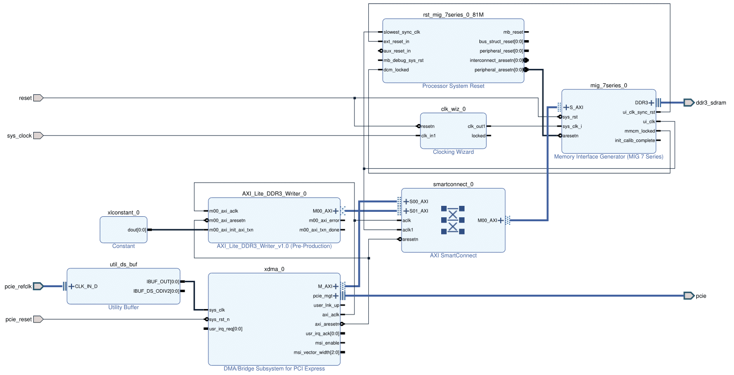
- AXI_DDR3_Writer is the custom IP block
- It takes the same 250MHz clock that the DMA Bridge generates
- It connects to a slave port on the AXI smart connect
- It takes a constant 1 value for the axi_init_axi_txn port, which means it always wants to initiatie an axi transfer(?)
24/10/2024 13:57
This design passes validation (meaning all the signals going to various ports are more or less what the port excpects).
However it does not pass syntehsis for reason:
[DRC MDRV-1] Multiple Driver Nets:
Net PCIe_DMA_i/AXI_DDR3_Writer_0/inst/UNCONN_OUT has multiple drivers:
PCIe_DMA_i/AXI_DDR3_Writer_0/inst/axi_awvalid_reg/Q, and
PCIe_DMA_i/AXI_DDR3_Writer_0/inst/AXI_DDR3_Writer_v1_0_M00_AXI_inst/axi_awvalid_reg/Q.
[DRC MDRV-1] Multiple Driver Nets:
Net PCIe_DMA_i/AXI_DDR3_Writer_0/inst/UNCONN_OUT has multiple drivers:
PCIe_DMA_i/AXI_DDR3_Writer_0/inst/axi_awvalid_reg/Q, and
PCIe_DMA_i/AXI_DDR3_Writer_0/inst/AXI_DDR3_Writer_v1_0_M00_AXI_inst/axi_awvalid_reg/Q.
which seems to indicate something is wrong with my code.